はじめに
以下の全3回に分けて、Adeiaの企業分析をおこなっていきます。今回は、技術紹介編です。Adeiaがライセンス提供するウェーハ接合技術、特にハイブリッドボンディング技術がどのようなものか、紹介していきます。
*基礎編:そもそも、ウェーハ接合・ハイブリッドボンディングとは?その応用は?
(Adeiaの企業分析とは別枠)
沿革編:Adeiaのウェーハ接合IP事業がになるまでの沿革。
技術紹介編:Adeiaがライセンス提供するウェーハ接合技術、特にハイブリッドボンディング技術がどのようなものか
提携企業編:Adeiaが自社のハイブリッドボンディング技術をライセンス提供している企業を紹介
ライセンス提携
Canon
> Direct Bond Interconnect (DBI®) hybrid bonding portfolio licensed to Canon to enhance image sensors in its industry-leading products
> Direct Bond Interconnect (DBI®) hybrid bonding portfolio licensed to Canon to enhance image sensors in its industry-leading products
(November 18, 2020)
Xperi Inc. – Xperi Licenses DBI to Canon for CMOS Image Sensors
*
(Dec 19, 2024)
Adeia Enters into Multi-Year IP License Agreement with Canon | Adeia Inc.
Kioxia
> Kioxia continues to be a leader in the industries it serves with next-generation 3D NAND memory
(Mar 28, 2023)
Adeia Signs Long-Term Semiconductor Patent License Agreement with Kioxia – IMAPS 3D InCites Content Platform
LAPIS Technology(Rohm group)
> DBI® Ultra die-to-wafer hybrid bonding
> enable LAPIS to deliver a new generation of ASSPs and custom LSI ASICs
(May 04, 2022)
Xperi and LAPIS, a ROHM Group Company, Enter into Hybrid Bonding License Agreement | Adeia Inc.
Xperi Inc. – Xperi and LAPIS, a ROHM Group Company, Enter into Hybrid Bonding License Agreement
Micron
Xperi Inc. – Tessera and Micron Enter Into Technology License Agreement, July 21, 2006
Xperi Inc. – Tessera Technologies and Micron Technology Announce Execution of New Technology and Patent License Agreements, July 31, 2014
Xperi and Micron Enter Into License Agreement for Hybrid Bonding | Adeia Inc., February 23, 2022
OmniVision
Xperi Inc. – OmniVision Signs License Agreement with Ziptronix, February 22, 2017
Qorvo
> Hybrid bonding technology introduces new opportunities to optimize the architecture of the RF front-end semiconductor devices
(Feb 15, 2023)
Adeia and Qorvo Enter into Hybrid Bonding License Agreement | Adeia Inc.
Raytheon
> Ziptronix’s Direct Bond Interconnect (DBI ) technology with multilayer CMOS integrated circuit processes.
(31 March 2007)
Ziptronix DBI process enables 3D integration for Raytheon CMOS ICs | Military Aerospace
Samsung
(December 10, 2018)
XPERI Announces Settlement and New Patent License Agreement with Samsung | Adeia Inc.
SK hynix
> Agreement Includes a Technology Transfer of DBI Ultra for Next-Generation Memory
> DBI Ultra makes it possible to manufacture 8-, 12- and even 16-high chip stacks
(February 6, 2020)
Xperi Enters into New Patent and Technology License Agreement with SK hynix | Adeia Inc.
SkyWater Technology
> SkyWater and its customers will now have access to Adeia’s ZiBond® direct bonding and DBI® hybrid bonding technology and IP
> developing heterogeneous integration platform solutions in its Florida facility which also includes silicon interposer and fan-out wafer-level packaging (FOWLP) technologies.
> Fully automated SUSS XBS-200 Microbonder at SkyWater’s Florida site will be used for 200 mm ZiBond® and DBI® services.
(05/12/2022)
SkyWater Enters License Agreement with Xperi for Hybrid Bonding Technology – Skywater Technology
SMIC
SMIC子会社のLFoundry(Avezzano, Italy)に対してライセンス供与
(March 14, 2017)
Xperi Inc. – SMIC Signs License Agreement For Invensas’ DBI® Technology
Xperi Inc. – Invensas DBI Technology Now Available at SMIC
中芯国际-中芯国际联手Invensas推出DBI技术平台 (smics.com)
中芯国际-中芯國際聯手Invensas推出DBI技術平臺 (smics.com)
Sony
> ZiBond™, enables the industry’s lowest distortion for imaging systems utilizing backside illumination
(Feb 09, 2011)
Ziptronix Signs Licensing Agreement with Sony – IMAPS 3D InCites Content Platform
> Ziptronix Licenses DBI® Hybrid Bonding Patents to Sony for Advanced Image Sensor Applications
(Mar 19, 2015)
Ziptronix Licenses DBI® Hybrid Bonding Patents to Sony for Advanced Image Sensor Applications | 3D InCites
Tezzaron
> Ziptronix Licenses Direct Bond Interconnect (DBI®) and ZiBond® Patented Technologies to Tezzaron Semiconductor for Advanced 3D Memory and 3D Integrated Assemblies
Ziptronix Licenses DBI® and ZiBond® to Tezzaron | Tezzaron
Tezzaron, Ziptronix, and Invensas on Interconnectology | 3D InCites
Ziptronix Teams with Tezzaron and Novati Technologies to Accelerate Development of 3D ICs | Tezzaron
With the Acquisition of Ziptronix, Tessera Takes the 3D IC Plunge | 3D InCites
The People Who Make DBI Possible – 3D InCites
Tower Semiconductor
> license of Invensas ZiBond ® and DBI ® 3D semiconductor interconnect technologies.
> complements Tower’s manufacturing of its state of the art stacked wafer BSI sensor platforms for time of flight (ToF), industrial global shutter and other CMOS image sensors on 300mm and 200mm wafers.
(June 10, 2020)
Xperi and Tower Semiconductor Announce New License for 3D Stacked Image Sensor Technology | Adeia Inc.
UMC
> optimize and commercialize the ZiBond and DBI technologies for a wide range of semiconductor devices including image sensors, radio frequency (RF), MEMS, display drivers, touch controllers, SoC, analog, power and mixed-signal devices.
(August 2, 2018)
Xperi Partners With UMC to Support Production of Direct and Hybrid Bonding 3D Semiconductor Technologies | Adeia Inc.
YMTC
> a key enabling technology for current and future generations of high performance, high-capacity 3D NAND flash memory
(October 12, 2021)
Xperi Inc. – Xperi Licenses Hybrid Bonding Technology to Yangtze Memory Technologies Co., Ltd. (YMTC)
R&D cooperation
Fraunhofer
> work together to integrate Ziptronix Direct Bond Interconnect (DBI®) technology into Fraunhofer’s state of the art 300mm wafer production line and demonstrate DBI as the industry’s finest pitch, thinnest and lowest total cost-of-ownership 3D integration solution.
(October 29, 2015)
Xperi Inc. – Ziptronix and Fraunhofer IZM-ASSID Collaborate on Development of Low-Cost 3D Integration Solutions
Adeiaがライセンス提供するウェーハ接合技術
adeia.com/resources/introducing-zibond-and-dbi-technologies
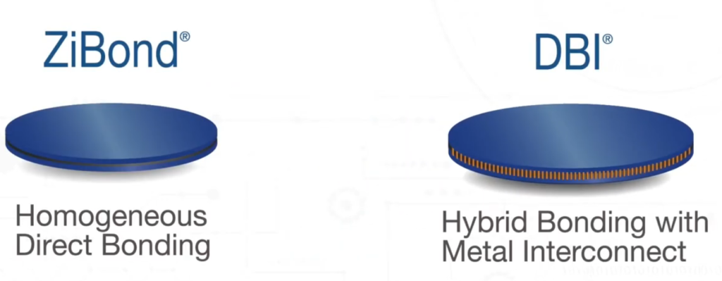
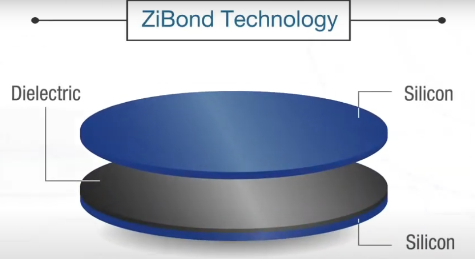
ZiBond®
ZiBond®は、ウェーハ同士の接合(Wafer-to-Wafer)に最適な低温直接接合技術です。熱膨張係数が同じまたは異なる半導体ウェハーやダイ間に強力な接合を形成します。この技術は、イメージセンサー、MEMS、さまざまなRFフロントエンドデバイスに適用されています。後述のDBIが接合と同時に電気的接続を確保しているのに対して、Zibondは電気的な接続ではない機械的な接合のみとなります。
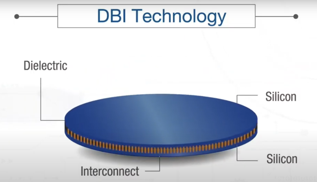
DBI®
DBI®は、ウェーハ同士の接合(Wafer-to-Wafer)に最適な低温ハイブリッドダイレクトボンディング技術です。前述のZiBond®が単純な接合であるのに対して、DBI®は電気的相互接続を伴う wafer-to-wafer ボンディングです。BSI Image Sensor, DRAM, MEMS, RFの製造プロセスに対して応用可能です。具体的なプロセスフローは以下の通りです。
- ウェーハ上の酸化シリコン(SiO2)等の誘電体層に、銅またはニッケルの埋め込み電極を形成する。
- ウェーハ表面をCMP(化学機械研磨)プロセスで研磨する。同時に、電極部分がわずかに凹む(ディッシング)。
- 表面をエッチングした後、窒素(N)を含むアンモニア系ガスで前処理を施す。
- 室温環境下で、2枚のウェーハの位置を金属電極が合うように調整(アライメント)し対向接触させると、向かい合う前処理済みの誘電体(SiO2など)同氏が共有接合し、永久接合が形成される。
この際、金属電極間は前述のディッシングにより隙間が空いた状態となる。 - 室温以上の比較的低温でのバッチアニール後、向かい合う金属電極の両端が熱膨張して接触し、接合界面で相互拡散することで、金属配線接合が形成される。
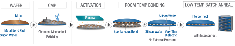
Dbi Wafer-to-Wafer Hybrid Bonding (adeia.com)
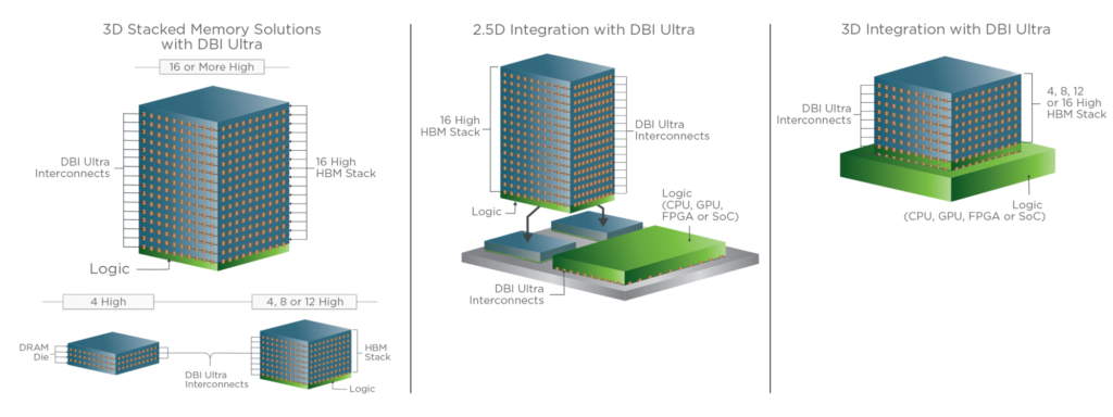
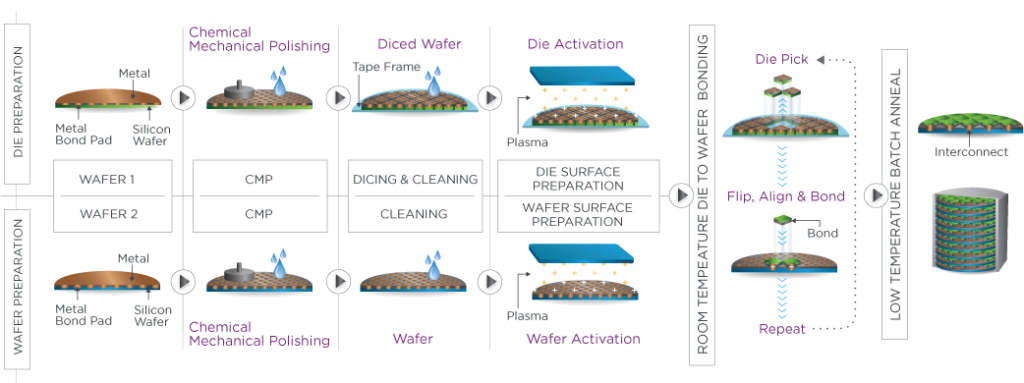
DBI® Ultra
DBI® Ultraは、ダイとウェーハ同士の接合(Die-to-Wafer)およびダイ同士の接合(Die-to-Die)のハイブリッドボンディング技術です。銅ピラーやアンダーフィルを不要にすることで、従来のアプローチと比較して飛躍的に薄いスタックを可能にします。また、1 µmインターコネクトピッチまで容易に微細化しながら、同一または異なるサイズのダイ、微細または粗いウェーハプロセス技術ノードで処理されたダイ、同一または異なるウェーハサイズで製造されたダイのスタッキングを可能にします。
応用先としては、DRAM、マイクロプロセッサ、グラフィックス・プロセッサ、SoCなどの大型ダイに適しています。特に、4、8、12、16ダイ以上の高帯域幅メモリー(HBM)スタック、高性能コンピューティングのためのCPU、GPU、FPGA、SoCとメモリーの2.5D/3D統合に応用が可能です。また、既知の良品ダイを他の既知の良品ダイにボンディングすることができ、高歩留まりのマルチダイスタック2.5Dおよび3Dアセンブリを可能にします。
具体的なプロセスフローは以下の図に示す通りです。基本的なプロセスは前述のDBI®と同じですが、DBI® Ultraではダイ(Die, チップ個片)の切り出し工程およびフリップ・アライン工程が含まれます。
DBI Die-to-Wafer Hybrid Bonding (adeia.com)
文献・特許
Low Temperature Hybrid Bonding for Die to Wafer Stacking Applications
コメント