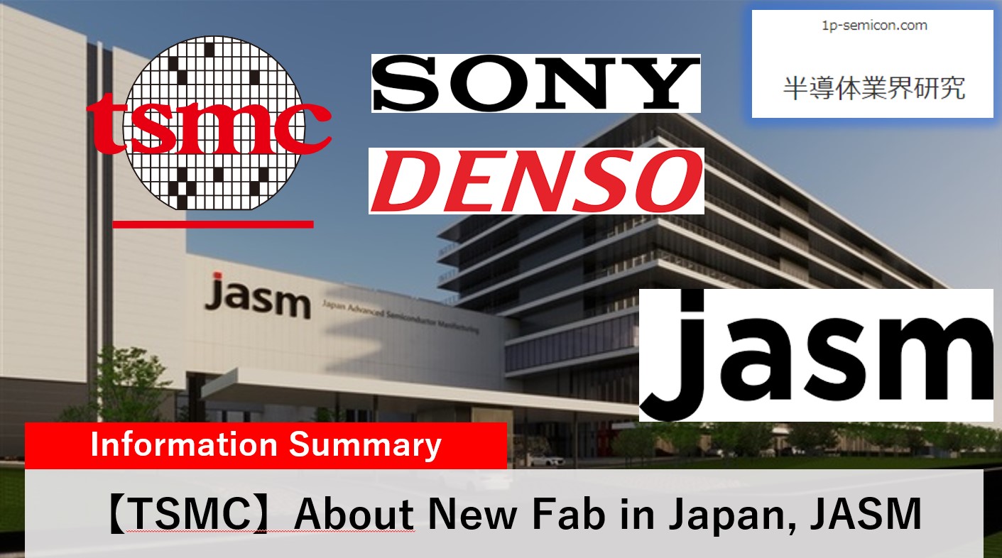
Introduction
This article provides basic information on “Japan Advanced Semiconductor Manufacturing Corporation“, commonly known as “JASM“. JASM is a subsidiary of TSMC, a major Taiwanese semiconductor contract manufacturer, which is currently constructing a plant in Kumamoto.
In this article, I have compiled information that is generally available to the public, such as the parent company TSMC, the background of JASM’s establishment, and information on employment opportunities. Since this is a compilation of articles and literature based on objective facts, I have not expressed any personal subjective opinions. However, some inferences from multiple objective facts may be included.
This article is an English version of the following article.
Basic Information of JASM
Company Profile
Company name :Japan Advanced Semiconductor Manufacturing, inc
Location:3802-14 Haramizu, Kikuyo-cho, Kikuchi-gun, Kumamoto, Japan
Establishment :December 10th, 2021
CEO :Yuichi Horita
Business :Foundry, manufacturing and sales of semiconductor devices, etc.
Number of Employees :Unknown
Capital stock :2,878.75 million yen
Major Shareholders :
Taiwan Semiconductor Manufacturing Corporation (TSMC)
Sony Semiconductor Solutions
Denso Corporation
About jasm
The following is an introduction to JASM as described in the application guidelines.
Japan Advanced Semiconductor Manufacturing Corporation (“JASM”) is a majority-owned subsidiary of TSMC and Sony Semiconductor Solutions Corporation (“SSS”) jointly announced in November 2021, located in Kumamoto Prefecture, Japan. JASM will provide contract manufacturing services starting with 22/28nm and 12/16nm FinFET processes to meet the strong global demand for semiconductors, and SSS will participate in JASM as a minority shareholder. In February 2022, Denso Corporation announced that it will make a minority investment of approximately 40 billion yen. Construction of JASM’s foundry in Japan is scheduled to begin in 2022, with the aim of starting production by the end of 2024. The foundry is expected to create approximately 1,700 new jobs for advanced technology professionals and have a monthly production capacity of 55,000 wafers (300mm wafers). The construction of the foundry in Japan is another step in TSMC’s long history of contributions to the Japanese semiconductor ecosystem since the establishment of its first Japanese subsidiary in 1997. Most recently, TSMC established a design center in Japan in 2019 to serve customers worldwide. In addition, TSMC is currently working with Japanese partners on advanced packaging technologies at the TSMC 3DIC R&D Center in Ibaraki, Japan.
出典:Japan Advanced Semiconductor Manufacturing株式会社 募集要項
The above information can be summarized in bullet points as follows.
- Plan announced: November 2021
- Shareholders of JASM:
TSMC (majority shareholder)
Sony Semiconductor Solutions Corporation (less than 20% shareholder)
Denso Corporation (over 10% shareholder) - Main Products: Logic semiconductors (22/28nm process and 12/16nm FinFET process)
- Production capacity: 55,000 wafers/month (12-inch, 300 mm wafer equivalent)
- Total number of employees: 1,700
- Operation Plan:
April 2022 – Start of construction
September 2023 – Construction to be completed (equipment start to be delivered)
End of 2024: Start of production
Makoto Onodera, President and Representative Director of TSMC Japan, also commented on JASM as follows.
Outside of Taiwan, the company’s overseas factories are located in the U.S., China, and Singapore, and Japan is the fourth country for the company; it is unusual for a new investment to start with a legacy node such as 22/28nm and the first time for a 300mm line to be operated as a joint venture (with Sony investing a small amount). In addition to the new Kumamoto plant, the number of investment projects in Japan has been increasing in recent years, including collaboration with the University of Tokyo, the opening of a design center in the Minatomirai area, and the establishment of a base for advanced package development in Tsukuba, which has become increasingly tinged as an important region for development and production.
出典:”特別インタビュー TSMCジャパン(株) 代表取締役社長 小野寺誠氏”, 電子デバイス産業新聞 より
Yuichi Hotta, president of JASM, has also set a goal of 50% procurement of equipment and materials in Japan. In addition, the company will use 100% renewable energy for electricity and recharge the same amount of groundwater used.
About TSMC, the parent company of JASM
Company Profile
Company name :Taiwan Semiconductor Manufacturing Co., Ltd.
台湾積体電路製造股份有限公司(繁: 台灣積體電路製造股份有限公司)
Location of HQ:No. 8, Li-Hsin Road 6 Hsinchu Science Park Hsinchu, 300 TWN
foundation :1987年2月代表者 :Dr. C.C. Wei, Ph.D.
Businesss :Foundry, manufacturing and sales of semiconductor devices, etc.
Number of Employees :about 65,000 (2021年)
Capital stock :259,303,804,580 Taiwan dollar(2022年)
Summary of TSMC
Taiwan Semiconductor Manufacturing Company, Ltd. (TSMC) is the world’s largest semiconductor foundry headquartered in Taiwan. As a specialized foundry manufacturer that only manufactures semiconductors, TSMC is responsible for the manufacture of semiconductors for device manufacturers around the world.
In 1987, Morris Chang, the founder of TSMC, established TSMC, the industry’s first dedicated foundry, at the request of the Taiwanese government. At the time, the semiconductor industry was dominated by vertically integrated device manufacturers (IDM), in which a single company handled everything from design to manufacturing and sales. However, the huge capital investment required to build a semiconductor manufacturing plant (fab) in this IDM structure stifled innovation by engineers with great ideas for circuit design and advanced architecture. Mr. Chang recognized this problem and decided that by separating the design and sales of chips from the manufacturing of chips and making each a specialized business (horizontal division of labor), he could develop both these companies and the semiconductor industry. Thus, TSMC became a pioneer in the horizontal division of labor as a foundry specializing in manufacturing, and became a central player in the now mainstream business model of the horizontal division of labor in semiconductors.
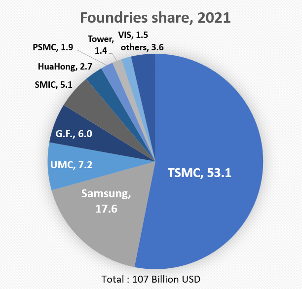
TSMC manufactures 12,302 products using 291 different technologies for 535 customers as of 2021. Its customers include many of the world’s leading logic IC manufacturers, such as Qualcomm, AMD, and Nvidia, and Japanese companies Sony and Renesas have also outsourced the manufacture of some of its products. TSMC’s high level of manufacturing technology has not allowed other foundry manufacturers to follow suit, with TSMC alone accounting for 53% of the foundry market share in fiscal year 2021.
TSMC’s connection with Japan
TSMC’s ties to Japan began with the establishment of its Japanese subsidiary in 1997, and the company has established various bases up to the present. The names of the bases and the year of establishment are as follows
1997年:TSMC Japan, a Japanese subsidiary, is established.
2019年:TSMC Japan Design Center and TSMC Design Technology Japan Corporation established
2019年:Established the System Design Center (a.k.a. d.lab) in partnership with the University of Tokyo
2021年:TSMC Japan 3DIC R&D Center established
2021年:Japan Advanced Semiconductor Manufacturing eatablished
2022年:Establishment of Osaka base office of TSMC Japan Corporation (planned)
Takuya Yasui, the director of the TSMC Japan Design Center, commented on the role played by the TSMC Japan Design Center.
TSMC Design Technology Japan is located in the Minato Mirai district of Yokohama and was established in January 2020. The role of the company is to support customers using 5nm, 3nm and beyond state-of-the-art processes by working as one team with the Taiwan headquarters and 7 design centers around the world. Specifically, the role will be to contribute to the development of design platforms by taking charge of block design using standard cells, SRAM memory, and the latest automated placement and routing tools, as well as the creation of design environments.
出典:”誠実かつ信頼を理念に最先端プロセスを通じて顧客とマーケットを結ぶ”, 日経クロステック より
The mission of the System Design Center (a.k.a. “d.lab”) is described in the University of Tokyo’s news release accompanying the establishment of the center as follows
A dedicated area-specific chip, in which unnecessary circuits are eliminated to focus on a specific area, can improve energy efficiency by an order of magnitude compared to a general-purpose chip. This is why IT companies around the world are embarking on the development of their own semiconductors. It is necessary to design the entire system and then translate this into an advanced semiconductor device.
出典:”東京大学・TSMC先進半導体アライアンス共同記者発表会”, 東京大学ニュースリリース より
However, it is not uncommon for the development of a specialized, domain-specific chip to take more than a year and involve several hundred people. Therefore, it is necessary to change chip development from the traditional capital-intensive approach to a knowledge-intensive approach. Creating knowledge-intensive chip design methods is an important mission of d.lab.
Commenting on the role of the TSMC Japan 3DIC R&D Center, Mr. Yutaka Emoto, Vice President and General Manager of the 3DIC R&D Center, said, “The 3DIC R&D Center will be responsible for the development and manufacturing of 3DICs in Japan.
TSMC Japan 3DIC R&D Center was established in March 2021 and has a laboratory and clean room on the premises of the National Institute of Advanced Industrial Science and Technology (AIST) in Tsukuba, Japan. Its mission is to develop technologies to cost-effectively realize SoCs with high performance and high functionality by combining semiconductor chips (chiplets) of different process nodes in a three-dimensional manner. We are also conducting R&D in collaboration with Japanese companies that have functional materials and elemental technologies.
出典:”誠実かつ信頼を理念に最先端プロセスを通じて顧客とマーケットを結ぶ”, 日経クロステック より
Background of JASM Establishment
Attraction of TSMC by the Japanese Government
Our modern lives are supported by digital services and industries such as AI, robots, smartphones, PCs, and cloud computing. In such a society, semiconductors are key components that can be regarded as its heart.
The shortage of semiconductors caused by various factors in recent years has had a major impact on manufacturing in industries that use semiconductors. This has made the stable procurement of semiconductors a challenge. In addition, the growing importance of semiconductors as a strategic material, essential in a wide range of industries, against a background of national conflicts, has led to calls for the strengthening of the domestic semiconductor supply chain from an economic security perspective.
The semiconductor supply chain consists mainly of the manufacturing equipment, materials, and device industries. Japan is strong in the manufacturing equipment and materials industries and boasts a high global market share. On the other hand, in the device sector, there are still players in Japan that can compete in the global market in memory, sensors, and power devices, or foreign companies already have manufacturing bases in Japan, but Japan lags behind in logic semiconductor manufacturing technology. Most of Japan’s logic semiconductor manufacturing technology is pre-40nm process technology and does not have the capacity to manufacture advanced logic semiconductors in the 20nm range and beyond. In other words, the supply chain can be made more robust by filling in the missing manufacturing base for advanced logic semiconductors in Japan’s domestic semiconductor industry.
However, manufacturing advanced semiconductors requires not only specialized equipment but also manufacturing process know-how, and building this know-how requires considerable time. This is why we decided to attract TSMC, which already has mature manufacturing technology and know-how in advanced logic semiconductors, with government assistance.
The above is a brief summary of items related to the attraction of TSMC in the semiconductor strategy of the Ministry of Economy, Trade and Industry’s Semiconductor and Digital Industry Strategy Study Council.
Certified Specific Semiconductor Production Facility Development Plan; Ministry of Economy, Trade and Industry
The “Certified Specific Semiconductor Production Facility Development Plan” was established by the Minister of Economy, Trade and Industry for the purpose of providing subsidies and other new measures to certified businesses that produce specific semiconductors. Logic semiconductors and memory semiconductors fall under the category of specified semiconductors, and the following specific conditions are set. In addition, the plan to be certified requires continuous production for 10 years or more and increased production when demand is tight.
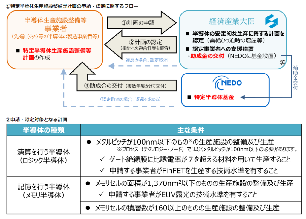
The grants will be made from a specific semiconductor fund totaling 617 billion yen placed at the New Energy and Industrial Development Organization (NEDO). Of this amount, a maximum of 476 billion yen will be granted to JASM, with the remainder of 92.93 billion yen going to the joint venture between Kioxia and Western Digital, and 46.47 billion yen to Micron Memory Japan.
Sony’s Investment and Aim
On February 15, 2022, TSMC and Sony Semiconductor Solutions Corporation (“SSS”) jointly announced that they will acquire less than 20% of JASM by investing approximately US$500 million (approximately 57 billion yen*) in capital. Mr. Terushi Shimizu, President and CEO of SSS, commented on the announcement:
As the global semiconductor shortage continues, we hope that this partnership with TSMC will contribute to the stable procurement of logic wafers not only for our company, but for the entire industry. We believe that further strengthening and deepening our partnership with TSMC, which possesses the world’s most advanced semiconductor production technology, will be of great significance to the Sony Group.
出典:”TSMCによる半導体ファウンドリの日本での設立と、ソニーセミコンダクタソリューションズによる少数持分出資について”, ソニーセミコンダクタソリューションズグループ ニュースリリース より
Mr. Shimizu, CEO of SSS, cited three objectives for the investment in JASM: “stable procurement of logic semiconductors,” “strengthening technical collaboration with TSMC,” and “contribution to strengthening the supply chain in Japan.
The stacked CMOS image sensor (hereinafter referred to as “CIS”), SSS’s mainstay product, consists of two layers: a pixel section that captures light and converts it into electrical signals, and a logic circuit section that converts the electrical signals into digital information and processes the information. The investment in JASM and the production of CISs are expected to solve the problem of “stable procurement of logic semiconductors”. The investment in JASM and its manufacturing are believed to be aimed at solving the issue of “stable procurement of logic semiconductors.
DENSO’s Investment and Aim
On February 15, 2022, TSMC, Sony Semiconductor Solutions and DENSO jointly announced that DENSO will make a minority investment of approximately US$350 million (approximately 40 billion yen*) in JASM. Through this investment, Denso has acquired a stake of more than 10% in JASM. Mr. Katsunori Nakamura, Representative Director of Denso Corporation, commented on the announcement:
Semiconductors are becoming increasingly important in the automotive industry amid the technological evolution of mobility, such as automated driving and electrification. Through this partnership with TSMC, we hope to achieve stable procurement of automotive semiconductors over the medium to long term and contribute to the automotive industry as a whole.
出典:”デンソーによる、JASMへの少数持分出資について”, 株式会社デンソーニュースリリース より
Denso’s investment this time targets 28-nanometer products, which are believed to be used in microcontrollers for electronic control units (ECUs) and other applications. In its basic semiconductor strategy, Denso aims to achieve both performance improvement and function development of in-vehicle semiconductors and stable procurement, and it is believed that JASM will manufacture 28nm products, the most advanced node of in-vehicle microcontrollers.
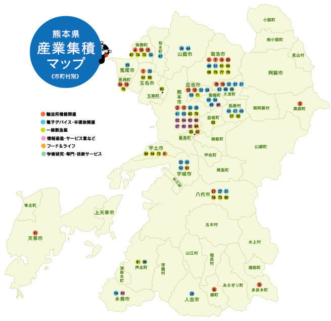
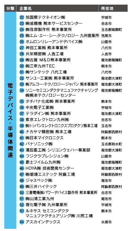
Impact on Kyushu Region and Kumamoto Prefecture
Kyushu Silicon Island
Since the 1960s, semiconductor companies have been locating factories in the Kyushu region, which has come to be known as the “Silicon Island. Currently, more than one-third of Japan’s semiconductor companies are concentrated in Kyushu.
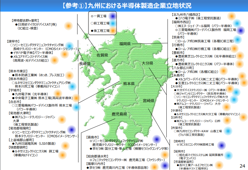
Kumamoto Prefecture and the Semiconductor Industry
Kumamoto Prefecture, where the new plant will be built, is home to Sony Semiconductor Manufacturing, Tokyo Electron, and other semiconductor-related companies. Water is essential for semiconductor manufacturing, and Kumamoto’s abundance of water resources is one of the reasons for the concentration of semiconductor companies.
Economic impact and revitalization of surrounding areas
Kyushu Financial Group, which owns Higo Bank in Kumamoto, has made an estimate of the economic ripple effect in Kumamoto Prefecture associated with the establishment of JASM and related companies moving into Kumamoto. According to the estimate, the effect is estimated to be approximately 2.4 trillion yen in the five years from 2025, after the start of operations, and approximately 4.3 trillion yen in the 10 years from 2022 to 2031. In addition, the impact on Kumamoto Prefecture’s gross domestic product is expected to be about 200 billion yen annually, which will have the effect of raising the level of growth by about 3%.
In addition, according to the 2022 roadside land prices announced by the National Tax Agency on July 1, 2022, the assessed value of “Hikari no Mori 3-chome Prefectural Road Sumiyoshi Kumamoto Line” in Kikuyo Town, Kumamoto Prefecture, increased by 5.0% over the previous year.
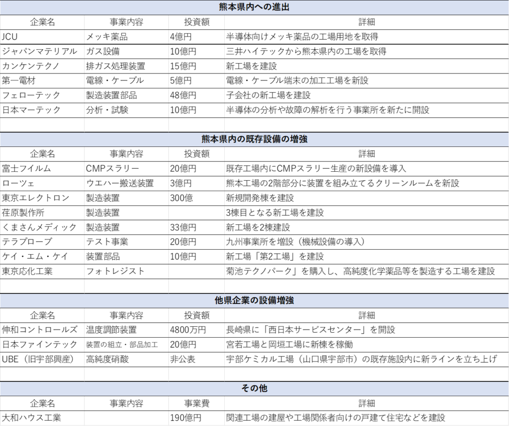
Expansion of affiliated companies’ facilities and entry into Kumamoto Prefecture
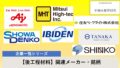
With the establishment of JASM, a number of related companies have been expanding their facilities and expanding or establishing plants in Kumamoto Prefecture. The table below summarizes the movements of some of the related companies that have been reported at this time. In addition to the companies listed here, several other companies have also decided to expand their facilities or advance into Kumamoto.
Recruitment information
Staffing Plan
JASM plans to secure approximately 1,700 personnel for operation by the end of 2024. This will consist of approximately 320 employees on loan from TSMC in Taiwan, 200 from Sony, 700, half of whom will be new graduates and half of whom will be new mid-career hires, and the remaining 500 will be outsourced personnel supply.
New Graduate Recruitment
The requirements for the hiring of new graduates to join the company in 2023 are as follows The overall number of recruits is approximately 100.

In addition, interviews are basically conducted entirely in English, with a total of three interviewers, two of whom are from TSMC’s head office (HR and engineering), plus an interpreter, and last approximately one hour. Regarding the required English proficiency, applicants will be evaluated on their willingness to take on the challenge of communicating in English. During the interview, you will also give a slide presentation of your research and be asked technical and mind-set questions about the content. In addition, the second half of the interview is an overview of the company and the offer, followed by a question-and-answer session.
Mid-Career Recruitment
As for mid-career recruiting, TSMC seems to be recruiting on various job sites in addition to TSMC’s recruiting page and Linkdin. In addition to new graduates, there is a wide range of positions available, including human resources and manager positions. The hard skills required are expertise, the ability to communicate effectively within the company, and the desire to improve language skills. Compensation is set in the following ranges depending on years of experience.
3 to 8 years of experience: 6 to 10 million yen
8 to 10 years of experience: 9 to 12 million yen
Training in Taiwan
After joining the company, employees will receive 6 to 9 months of training at the training center in Taichung City, Taiwan (exact training period varies depending on the assignment). For employees on loan from Sony, a firm commitment to Taiwan is scheduled to begin in the fall of 2022 or later in order to acquire TSMC-style factory operation know-how and work procedures. Practical training will be provided at the training center using the same equipment that will be installed at the Kumamoto plant.
Conclusion
I will revise the contents of this article as necessary as soon as I find errors or other inaccuracies. In particular, there may be errors in my own understanding regarding the section on the Japanese government’s attraction of TSMC.
Thank you for reading to the end.
References
【JASMの基本情報】
- Japan Advanced Semiconductor Manufacturing(株)-マイナビ2023
- Japan Advanced Semiconductor Manufacturing株式会社 2023年卒向け募集要項
- TSMCの技術系新卒採用
- 特定半導体生産施設整備等計画の概要
- “特別インタビュー TSMCジャパン(株) 代表取締役社長 小野寺誠氏”, 電子デバイス産業新聞, 2022/01/07
- “TSMC熊本工場、国内調達5割へ「サプライヤーの投資必要」”, 日本経済新聞, 2022年8月23日
【親会社のTSMCについて】
- 台湾セミコンダクター・マニュファクチャリング【TSM】:企業情報/株価 – Yahoo!ファイナンス, Yahoo! Japan.
- Sahil Bloom, “The Amazing Story of Morris Chang”, The Curiosity Chronicle, Jan 25, 2021
- 吉川明日論, “半導体業界のレジェンド、TSMC創業者Morris Chang物語”, TECH+, 2021/03/11
- TSMC-会社情報
- TSMCデザインテクノロジージャパン(株) – マイナビ2023
- “TSMC日本法人、大阪に事務所設置へ/台湾”, The News Lens, 2022/09/06
- “TSMCジャパン3DIC研究開発センターがオープン”, EE Times Japan, 2022/06/27
- “東京大学・TSMC先進半導体アライアンス共同記者発表会”, 東京大学, 2019/11/27
- “東京大学とTSMCがアライアンス締結”, EE Times Japan, 2019/11/28
- “誠実かつ信頼を理念に最先端プロセスを通じて顧客とマーケットを結ぶ”, 日経クロステック
【JASM設立の経緯】
- “半導体・デジタル産業戦略検討会議”, 経済産業省
- “特定高度情報通信技術活用システムの開発供給及び導入の促進に関する法律(特定半導体生産施設整備等関係)”,経済産業省
- “認定特定半導体生産施設整備等計画”,経済産業省
- “特定半導体基金事業”, NEDO(新エネルギー・産業開発機構)
- “積層型CMOSイメージセンサーの生みの親が語る、世紀の発明を支えた論理的思考”, ソニーセミコンダクタソリューションズグループ, 2022/09/21
- “2022年度 事業説明会 イメージング&センシング・ソリューション分野 説明資料”, ソニーグループ, 2022/05/26
- “デンソーによる、JASMへの少数持分出資について”, 株式会社デンソーニュースリリース, 2022年2月15日
- “半導体戦略説明会”, 株式会社デンソー, 2022年6月1日
- “台湾における半導体産業について-台湾の関連政策と主要企業のサプライチェーン調査”, 日本貿易支援機構(ジェトロ)海外調査部, 2022年5月
【九州・熊本県への影響】
- “”シリコンアイランド九州の復活に向けて~2030年の日本社会を支える九州であり続けるために~”, 九州産業局”, 2022年5月19日
- TSMCの技術系新卒採用
- 熊本企業立地ガイド/熊本県産業集積マップ
- “熊本TSMC進出の波紋とその衝撃(前)”, NetIB-News, 2022年9月2日
- “荏原製作所 熊本事業所に新工場を建設/デンソーTSMC工場へ事業出資へ”, REGIONAL CAREER 熊本, 2022.02.24
- “株式会社テラプローブ が芦北町の九州事業所を増設!”, 企業立地ガイド熊本, 2022年1月27日
- “株式会社ケイ・エム・ケイが市と立地協定~今秋操業開始、45人新規雇用へ”, 宇城市, 2022年03月31日
- “東京応化工業株式会社、菊池市の工場の新設を決定!”, 企業立地ガイド熊本, 2022年3月9日
- “TSMCが呼び水に 半導体関連企業、九州に進出相次ぐ”, 日本経済新聞, 2022年7月9日
- “ローツェ、九州工場の生産増強 半導体需要拡大で”, 日本経済新聞, 2022年7月13日
- “JCU、熊本で半導体関連の工場用地取得 メッキ薬品”, 日本経済新聞, 2022年9月2日
- “大和ハウス、TSMC工場周辺を集中開発 190億円規模”, 日本経済新聞, 2022年10月7日
- “半導体関連の伸和、長崎に新拠点 精密空調の保守強化”, 日本経済新聞, 2022年7月8日 11:30
- “日本ファインテック 福岡で半導体向け大型投資”, 日本経済新聞, 2022年9月22日
- “富士フイルム社長「半導体SC強化」 熊本で研磨剤生産”, 日本経済新聞, 2022年9月12日
- “フェローテックHD、48億円投じ熊本に半導体関連新工場”, 日本経済新聞, 2022年5月23日
- “台湾のTSMC進出で“10年間に4兆3千億円の経済効果””, NHK NEWS WEB, 2022/09/07
- “TSMC操業5年で経済効果2.4兆円 九州FG試算”, 西日本新聞, 2022/9/8
【採用情報】
コメント